
ASML
Introduction
- Do you want to master the entire patterning process?
- Do you want to help define the next generation of patterning systems?
- Would you like to work with the world’s leading patterning scientists and engineers?
- Will you enjoy creating the future?'
Then join the ASML Applications Engineering department!
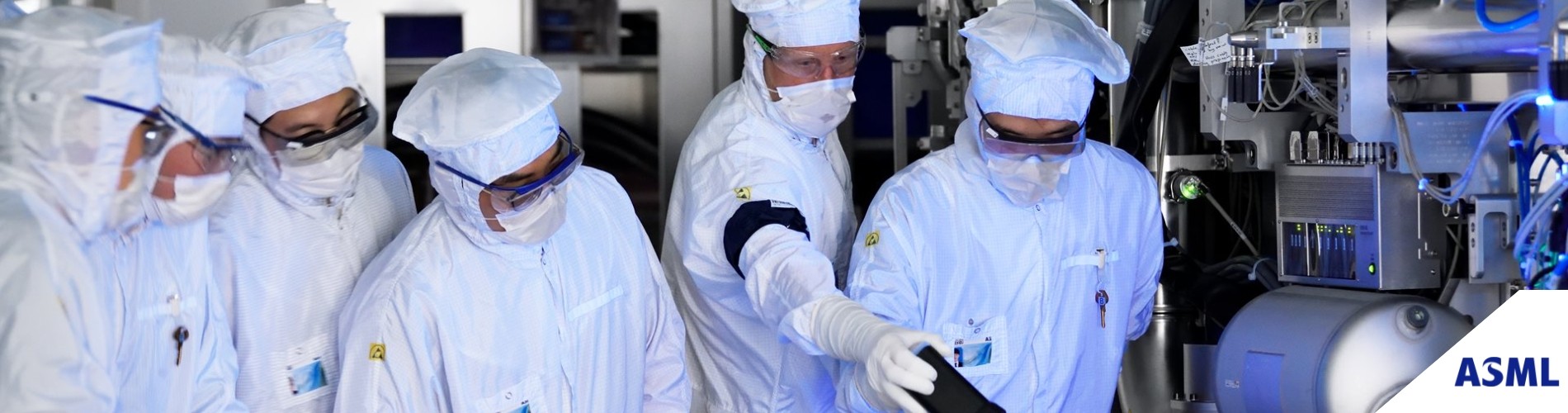
As an Application Engineer, you work with the most senior level of engineers and the elite scientists of ASML’s customers. You are therefore in the perfect position to determine what our customers want and you translate this understanding of the customer to ASML development teams to help define future generations of ASML products. You will be shaping the future of the chip fabrication.
Job Mission
The Applications Engineering department at ASML maximizes the wafer yield at customer fab plants. It achieves this goal not only by optimizing the lithography process, but also by optimizing the entire chain of processes that are required in chip patterning (i.e. lithography, developing, etching, ashing, deposition, and coating). It also achieves this goal by optimizing metrology and inspection.
You will be defining the future of chip patterningThe Applications Engineering department has around 50 consultant engineers working in teams of six or seven people. Each team is dedicated to specific ASML customers. The teams consult with the customer’s top scientists and engineers to identify opportunities for improvement – these improvements may be hardware based or software based or both, and they can be located anywhere in the patterning process. When an opportunity is identified, and if the customer agrees, that’s where you come in to specify the improvement.
You will:
- Work within the customer project team supporting the development and integration of solutions with the goal to meet customer requirements;
- Develop applicable competencies within the Application Engineering department: big data, statistics, analysis toolkits, lithographic processing and metrology;
- Execute root-cause identification analysis on the customer data analysis and identify solutions for improvements;
- Work on customer tools and in customer environment to proof own developed solutions to be beneficial for on product performance;
- Be able to drive new product definition by understanding customer requirements and position them within the customer production eco-system.
Master degree in Physics, Mathematics or Engineering, preferably in the domain of nanotechnology, optics or semiconductor industry.
For this position you have:
- 2+ years of applications/on-product performance/semiconductor process engineering experience in the area of lithography, patterning (pattern transfer) or metrology;
- Tangible experience in process integration or semiconductor device manufacturing especially in the domains of overlay, imaging. focus, metrology or defectivity related to node/process development;
- Proven ability to perform in a high stress and ambiguous environment while always
maintaining focus on customer goals and relationships; - Excellent English language skills (both verbal and non-verbal)
- Previous experience with optimizing on-product performance of ASML equipment is a
plus.
- Strong analytical thinker (can easily “connect the dots”);
- Always showing independence & initiative;
- Customer focused;
- Decisive;
- Driven – never ever giving-up until the job is completely done;
- Can excel in a multi-cultural environment;
- Understanding the key differences between activity and accomplishment
- Ability to travel ~25%